Advanced semiconductor devices
 Advanced semiconductor devices
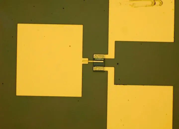
The “Advanced Semiconductor Devices” project is focused on the design and development of state-of-the-art devices using next-generation materials such as GaN (Gallium Nitride), SiC (Silicon Carbide), Ga2O3 (Gallium Oxide), and various 2D materials. This initiative aims to exploit the unique properties of these advanced materials to create semiconductor devices that surpass traditional silicon-based devices in aspects such as speed, efficiency, and tolerance to extreme environments.
Key Aspects of the Project:
TCAD Simulation for Various Materials: The project emphasizes TCAD (Technology Computer-Aided Design) simulations to predict the behavior of devices made from different advanced materials. This phase involves innovative design strategies to enhance multi-functionality and performance, optimizing device architecture for each material to improve electron mobility, reduce resistance, and achieve faster switching speeds, leading to enhanced energy efficiency and overall performance.
Advanced Fabrication Techniques Across Materials: The project explores new fabrication techniques for devices using GaN, SiC, Ga2O3, and 2D materials. This includes developing methods for producing layers of these materials with minimal defects and superior uniformity. Advancements in fabrication are key for the reliable performance of devices, ensuring consistency and quality in production.
Physical Mechanisms and Reliability in Diverse Materials: Investigating the physical mechanisms underlying the operation of devices made from these advanced materials is a crucial aspect. Understanding the physics of electron behavior, material properties, and thermal dynamics across different materials informs strategies for enhancing device reliability and longevity. This is vital for their application in high-power and high-frequency environments.
Circuit Integration and Diverse Applications: The project aims to integrate these advanced devices into high-frequency electronic circuits, expanding their application in areas such as wireless communication, radar systems, and satellite communications. These devices offer invaluable benefits in efficiency and speed for modern high-frequency applications, contributing to the advancement of electronic systems.
Future Directions: The project plans to continue refining technologies for various advanced semiconductor materials, exploring new design paradigms, and advancing fabrication techniques. The ultimate goal is to mainstream these advanced semiconductor devices for a broad spectrum of high-performance electronic applications, leading to more efficient and powerful electronic devices.
This initiative aligns with the global focus on advanced semiconductor technologies, underscoring their critical role in driving future electronic innovations.
My recent publications in this field:
- Advanced device design and fabrication
J.-K. Huang et al., “High-κ perovskite membranes as insulators for two-dimensional transistors,” Nature, vol. 605, no. 7909, pp. 262–267, May 2022, doi: 10.1038/s41586-022-04588-2.
Z. Wang et al., “A high-performance tunable LED-compatible current regulator using an integrated voltage nanosensor,” IEEE Transactions on Electron Devices, vol. 66, no. 4, pp. 1917–1923, Apr. 2019, doi: 10.1109/TED.2019.2899756.
- Device TCAD simulation
Z. Wang, “Proposal of a novel recess-free enhancement-mode AlGaN/GaN HEMT with field-assembled structure: a simulation study,” Journal of Computational Electronics, vol. 18, no. 4, pp. 1251–1258, Dec. 2019, doi: 10.1007/s10825-019-01383-7.
Z. Wang, D. Yang, J. Cao, F. Wang, and Y. Yao, “A novel technology for turn-on voltage reduction of high-performance lateral heterojunction diode with source-gate shorted anode,” Superlattices and Microstructures, vol. 125, no. September 2018, pp. 144–150, Jan. 2019, doi: 10.1016/j.spmi.2018.11.003.
- Device physics
Z. Wang, D. Yang, J. Shi, and Y. Yao, “Approaching ultra-low turn-on voltage in GaN lateral diode,” Semiconductor Science and Technology, vol. 36, no. 1, p. 014003, Jan. 2020, doi: 10.1088/1361-6641/abc70b.
Z. Wang and L. Li, “Two-dimensional polarization doping of GaN heterojunction and its potential for realizing lateral p–n junction devices,” Appl. Phys. A, vol. 128, no. 8, p. 672, Aug. 2022, doi: 10.1007/s00339-022-05824-2.
F. Wang, W. Chen, R. Sun, Z. Wang, Q. Zhou, and B. Zhang, “An analytical model on the gate control capability in p-GaN gate AlGaN/GaN high-electron-mobility transistors considering buffer acceptor traps,” Journal of Physics D: Applied Physics, vol. 54, no. 9, p. 095107, Mar. 2021, doi: 10.1088/1361-6463/abc504.
Zeheng Wang
CERC Fellow of Quantum Artificial Intelligence @CSIRO
My research interests include quantum machine learning, quantum computing devices, semiconductor devices, and applied artificial intelligence for electronics.